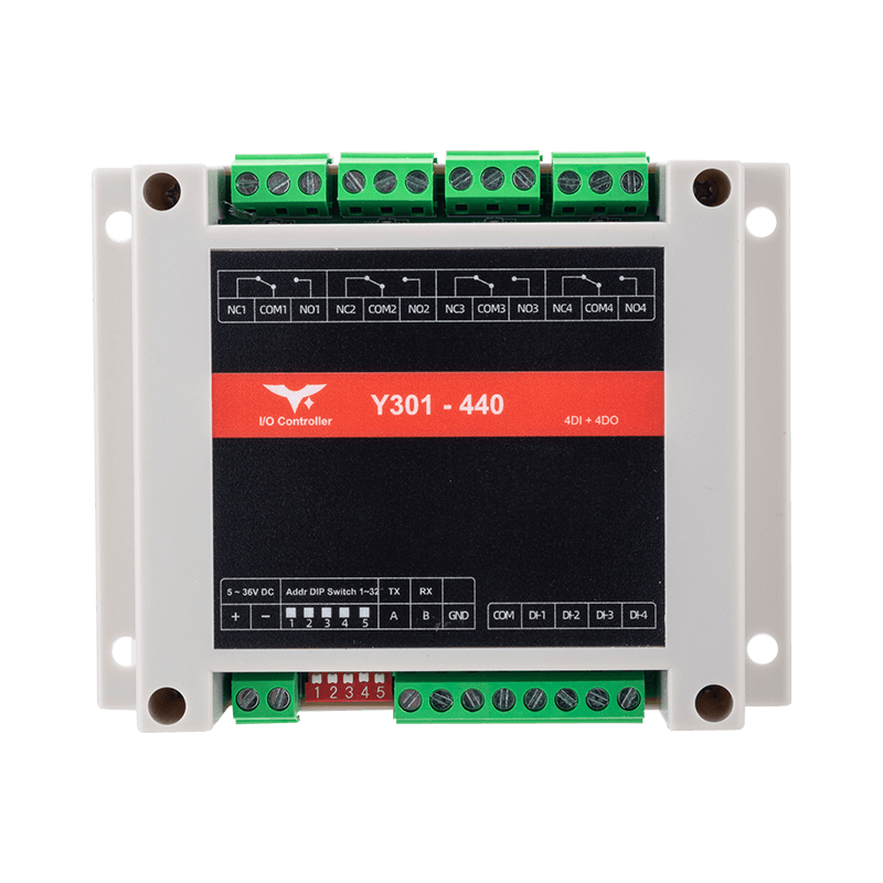
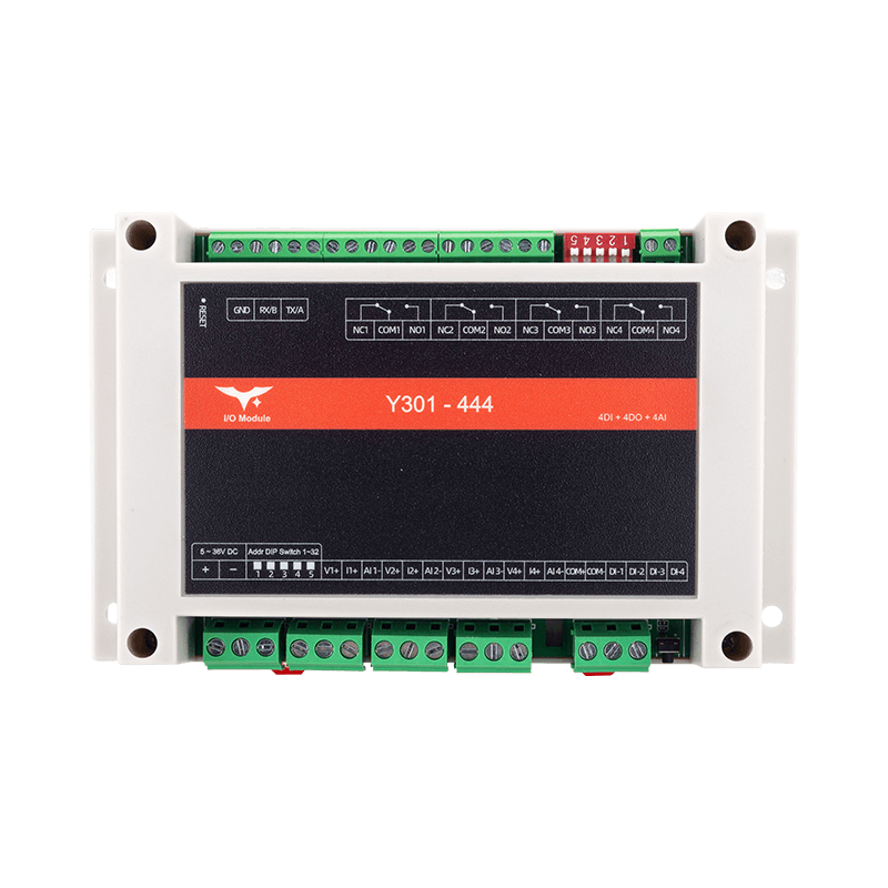
Appearance
Y301-440/444 Technical Manual
| Y301-440 | Y301-444 |
|---|---|
 |  |
Contents
- Overview
- Default Settings
- Modbus Register Map
- Command Examples
- Parameter Configuration
- Automation Rules
- Troubleshooting
1. Overview
This manual describes the Modbus RTU communication commands for the Y301-440 and Y301-444 I/O modules.
| Model | DI | DO | AI | Description |
|---|---|---|---|---|
| Y301-440 | 4 | 4 | 0 | Four inputs + four relays |
| Y301-444 | 4 | 4 | 4 | Four inputs + four relays + four analog inputs |
Frame format: [slave address][function code][data][CRC low][CRC high]
The examples below use slave address 0x01. Replace it with the actual device address in your application.
2. Default Settings
| Parameter | Default |
|---|---|
| Slave address | 1 |
| Baud rate | 9600 bps |
| Data bits | 8 |
| Parity | None |
| Stop bits | 1 |
3. Modbus Register Map
3.1 Digital Input (DI) - Function Code 0x02
| Channel | Address | Supported Models |
|---|---|---|
| DI1 | 0x0000 | Y301-440, Y301-444 |
| DI2 | 0x0001 | Y301-440, Y301-444 |
| DI3 | 0x0002 | Y301-440, Y301-444 |
| DI4 | 0x0003 | Y301-440, Y301-444 |
Return value: 0 = inactive, 1 = active.
3.2 Digital Output (DO) - Function Code 0x01/0x05
| Channel | Address | Supported Models |
|---|---|---|
| DO1 | 0x0000 | Y301-440, Y301-444 |
| DO2 | 0x0001 | Y301-440, Y301-444 |
| DO3 | 0x0002 | Y301-440, Y301-444 |
| DO4 | 0x0003 | Y301-440, Y301-444 |
Write value: 0x0000 = open, 0xFF00 = closed.
3.3 Analog Input (AI) - Function Code 0x04 (Y301-444 only)
| Channel | Address | Description |
|---|---|---|
| AI1 voltage | 0x0000 | Voltage value in mV |
| AI1 current | 0x0001 | Current value in uA |
| AI2 voltage | 0x0002 | Voltage value in mV |
| AI2 current | 0x0003 | Current value in uA |
| AI3 voltage | 0x0004 | Voltage value in mV |
| AI3 current | 0x0005 | Current value in uA |
| AI4 voltage | 0x0006 | Voltage value in mV |
| AI4 current | 0x0007 | Current value in uA |
Each AI channel can be wired for either voltage or current. The other reading is invalid.
3.4 Configuration Registers - Function Code 0x03/0x06
| Address | Parameter | Range | Default |
|---|---|---|---|
0x003E | Slave address | 1-255 | 1 |
0x0057 | Baud rate | 600-230400 | 9600 |
0x0059 | Data bits | 8 or 9 | 8 |
0x005A | Stop bits | 1 or 2 | 1 |
0x005B | Parity | 0=None, 1=Odd, 2=Even | 0 |
4. Command Examples
4.1 Read Digital Inputs
| Operation | Request (Hex) |
|---|---|
| Read DI1 | 01 02 00 00 00 01 B9 CA |
| Read DI2 | 01 02 00 01 00 01 E8 0A |
| Read DI3 | 01 02 00 02 00 01 18 0A |
| Read DI4 | 01 02 00 03 00 01 49 CA |
4.2 Read Digital Output Status
| Operation | Request (Hex) |
|---|---|
| Read DO1 | 01 01 00 00 00 01 FD CA |
| Read DO2 | 01 01 00 01 00 01 AC 0A |
| Read DO3 | 01 01 00 02 00 01 5C 0A |
| Read DO4 | 01 01 00 03 00 01 0D CA |
4.3 Control Digital Outputs
| Operation | Command |
|---|---|
| Open DO1 | 01 05 00 00 00 00 CD CA |
| Close DO1 | 01 05 00 00 FF 00 8C 3A |
| Open DO2 | 01 05 00 01 00 00 9C 0A |
| Close DO2 | 01 05 00 01 FF 00 DD FA |
| Open DO3 | 01 05 00 02 00 00 6C 0A |
| Close DO3 | 01 05 00 02 FF 00 2D FA |
| Open DO4 | 01 05 00 03 00 00 3D CA |
| Close DO4 | 01 05 00 03 FF 00 7C 3A |
4.4 Read Analog Inputs (Y301-444 only)
| Operation | Request (Hex) |
|---|---|
| Read AI1 voltage | 01 04 00 00 00 01 31 CA |
| Read AI1 current | 01 04 00 01 00 01 60 0A |
| Read AI2 voltage | 01 04 00 02 00 01 90 0A |
| Read AI2 current | 01 04 00 03 00 01 C1 CA |
| Read AI3 voltage | 01 04 00 04 00 01 70 0B |
| Read AI3 current | 01 04 00 05 00 01 21 CB |
| Read AI4 voltage | 01 04 00 06 00 01 D1 CB |
| Read AI4 current | 01 04 00 07 00 01 80 0B |
4.5 Quick Reference Table
| Operation | Request (Hex) |
|---|---|
| Read DI1 | 01 02 00 00 00 01 B9 CA |
| Read DI2 | 01 02 00 01 00 01 E8 0A |
| Read DI3 | 01 02 00 02 00 01 18 0A |
| Read DI4 | 01 02 00 03 00 01 49 CA |
| Open DO1 | 01 05 00 00 00 00 CD CA |
| Close DO1 | 01 05 00 00 FF 00 8C 3A |
| Open DO2 | 01 05 00 01 00 00 9C 0A |
| Close DO2 | 01 05 00 01 FF 00 DD FA |
| Open DO3 | 01 05 00 02 00 00 6C 0A |
| Close DO3 | 01 05 00 02 FF 00 2D FA |
| Open DO4 | 01 05 00 03 00 00 3D CA |
| Close DO4 | 01 05 00 03 FF 00 7C 3A |
5. Parameter Configuration
5.1 Change the Slave Address
Set the slave address to 5:
text
Request:  01 06 00 3E 00 05 E8 00
Response: 01 06 00 3E 00 05 E8 00
After the change, subsequent commands must use the new address.
5.2 Change the Baud Rate
Common baud-rate values:
| Baud Rate | Value |
|---|---|
| 9600 | 0x00002580 |
| 19200 | 0x00004B00 |
| 38400 | 0x00009600 |
| 115200 | 0x0001C200 |
Power-cycle the device after changing the baud rate.
5.3 Restore Factory Defaults
Hold the Reload button for 3-15 seconds to restore:
- Slave address ->
1 - Baud rate ->
9600 - All parameters -> factory defaults
6. Automation Rules
The Y301-440/444 support DI -> DO automation, and the Y301-444 also supports AI threshold triggering. Up to 8 rules are supported, with 2 rules per DO.
6.1 Automation Register Map
Rules start at address 0x0080. Each rule uses 8 registers (16 bytes).
| Offset | Field | Description |
|---|---|---|
+0 | Mode | Rule type (see table below) |
+1 | Action | 0=open, 1=close, 2=toggle |
+2 | DO index | Target relay, starting from 1 |
+3 | Trigger index | Source DI or AI, starting from 1 |
+4-5 | Parameter 1 | Mode-dependent, 32-bit |
+6-7 | Parameter 2 | Mode-dependent, 32-bit |
6.2 Rule Modes
| Mode | Name | Description |
|---|---|---|
| 0 | DI follow | DO follows the DI state |
| 1 | DI inverse | DO is the inverse of the DI state |
| 2 | Pulse | DO outputs a pulse for parameter1 ms when DI triggers |
| 3 | Delayed ON | DO closes parameter1 ms after DI closes |
| 4 | Delayed OFF | DO opens parameter1 ms after DI opens |
| 5 | Cycle | DO toggles periodically, parameter1=ON time, parameter2=OFF time |
| 9 | Daily schedule | Execute the action daily at the time specified by parameter1 (seconds since midnight) |
| 10 | AI threshold | Trigger when AI exceeds parameter1 (Y301-444 only) |
| 13 | Logic combination | Apply AND/OR/XOR logic across multiple DI channels |
6.3 Example: DO1 Follows DI1
Configuration:
| Field | Value |
|---|---|
| Mode | 0x0000 (DI follow) |
| Action | 0x0001 (close when DI=1) |
| DO index | 0x0001 |
| Trigger index | 0x0001 |
| Parameter 1 | 0x00000000 |
| Parameter 2 | 0x00000000 |
Modbus command:
text
01 10 00 80 00 08 10 00 00 00 01 00 01 00 01 00 00 00 00 00 00 00 00 0D FE6.4 Example: Close DO1 Daily at 18:00
Configuration:
| Field | Value |
|---|---|
| Mode | 0x0009 (daily schedule) |
| Action | 0x0001 (close) |
| DO index | 0x0001 |
| Trigger index | 0x0000 |
| Parameter 1 | 0x0000FD20 (64800 seconds = 18:00) |
| Parameter 2 | 0x00000000 |
6.5 Example: Close DO1 When AI1 Exceeds 5 V (Y301-444 only)
Configuration:
| Field | Value |
|---|---|
| Mode | 0x000A (AI threshold) |
| Action | 0x0001 (close) |
| DO index | 0x0001 |
| Trigger index | 0x0001 (AI1) |
| Parameter 1 | 0x00001388 (5000 mV) |
| Parameter 2 | 0x000003E8 (minimum trigger interval 1000 ms) |
7. Troubleshooting
| Symptom | Cause | Solution |
|---|---|---|
| No response | Wrong address or baud rate | Check settings and try broadcast address 0 |
| CRC error | Wiring issue or interference | Check RS485 polarity and add termination resistors |
| DO does not switch | Load exceeds rating | Reduce the load and verify contact ratings |
| DI always reads 0 | Wiring error | Check COM/DI wiring and input voltage |
| AI reading is abnormal | Wrong wiring mode | Verify voltage/current wiring; each channel supports only one mode at a time |
LED Indicators
| LED | Status | Meaning |
|---|---|---|
| POWER | Solid on | Power is normal |
| TX | Flashing | Data is being transmitted |
| RX | Flashing | Data is being received |
| DI1-DI4 | On | Input is active |
| DO1-DO4 | On | Relay is closed |
- Manufacturer: Hunan YenGear Tech Co., Ltd.
- Email: hi@yengear.com
- Website: www.yengear.com