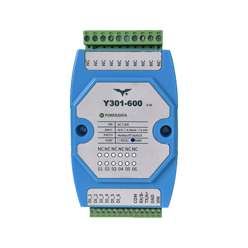
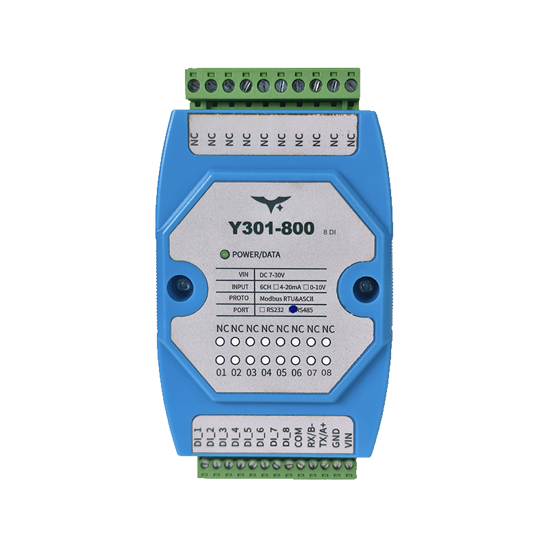
Appearance
Y301-600/800/G00 Digital Input Module Technical Manual
| Y301-600 | Y301-800 | Y301-G00 |
|---|---|---|
 |  | |
Manufacturer: Hunan Yanji Tech Co.,Ltd
Address: Room 21014, Unit 1, Fudixingguang Plaza, Yuhua District Yingxin Road, Changsha, Hunan, P.R. China
Email: hi@yanjiiot.com
Website: www.yanjiiot.com
Document Control
| Item | Detail |
|---|---|
| Version | V1.0.0 |
| Release Date | November 2025 |
| Applicable Models | Y301-600, Y301-800, Y301-G00 |
Table of Contents
- Introduction
- System Overview
- Modbus Communication Parameters
- Register Map
- Command Reference
- Configuration Workflow
- Diagnostics & FAQ
- Appendix
1. Introduction
This manual details the Modbus-oriented integration guide for the Y301-600/800/G00 digital input modules. All three variants inherit the DAM0800DI-YD opto-isolated hardware and share identical firmware; only the number of discrete input channels differs (6, 8, or 16). The content is intended for engineers who connect the modules to PLCs, SCADA platforms, industrial PCs, or custom telemetry gateways.
Key goals:
- Describe supported communication formats and addressing concepts.
- Provide definitive register mappings for DI status and configuration.
- Offer ready-made Modbus frames for commissioning and diagnostics.
- Capture field-proven troubleshooting steps found in the original Chinese manual.
2. System Overview
2.1 Hardware Summary
| Attribute | Detail |
|---|---|
| Supply Voltage | DC 7–30 V |
| Inputs | 6× DI (Y301-600) / 8× DI (Y301-800) / 16× DI (Y301-G00) |
| Isolation | Optocoupler isolation per channel |
| Input Modes | Dry contact or 3.3–24 V wet input |
| Installation | 120 × 70 × 35 mm enclosure, 35 mm DIN rail |
| Environment | -40 °C ~ +85 °C, 5–95 % RH non-condensing |
2.2 Communication & Addressing
- Interfaces: RS485 (default) or RS232 (factory variant). Both expose Modbus RTU/ASCII slave mode.
- Supported baud rates: 2400, 4800, 9600 (default), 19200, 38400 bps.
- Device addresses: 0–255 via software register. Broadcast address 254 (0xFE) is available for single-module debugging.
- Effective device address = offset address (software) + any DIP offset defined by the PCB (factory default offset 0).
- CRC-16 (Modbus) is required for all RTU frames. ASCII frames follow LRC validation per Modbus standard.
3. Modbus Communication Parameters
| Parameter | Value |
|---|---|
| Function Codes | 0x01 (Read Coils), 0x02 (Read Discrete Inputs), 0x03 (Read Holding Registers), 0x05 (Write Single Coil), 0x0F (Write Multiple Coils) |
| Frame Format | [Slave][Function][Payload][CRC Lo][CRC Hi] (RTU) |
| Default Frame Settings | 9600 bps, 8 data bits, no parity, 1 stop bit |
| Broadcast Behavior | Slave address 0xFE responds without CRC check from master; only recommended when one module is connected |
| Register Addressing | 0-based addressing inside packets; PLC-style addresses (1xxxx, 3xxxx, 4xxxx) map as described below |
3.1 Modbus Address Ranges
- 00001–09999 → Coils (typically DO, unused here but reserved for compatibility)
- 10001–19999 → Discrete Inputs (DI status)
- 30001–39999 → Input registers (mirrors of DI states where applicable)
- 40001–49999 → Holding registers (configuration parameters)
Address 10001 corresponds to Modbus register 0x0000 in the data field because Modbus packets use zero-based offsets.
4. Register Map
4.1 Discrete Inputs (Function 0x02)
| PLC Address | Modbus Offset (Hex) | Description | Models |
|---|---|---|---|
| 10001 | 0x0000 | DI1 status (bit0 of first byte) | All |
| 10002 | 0x0001 | DI2 status | All |
| … | … | … | … |
| 10006 | 0x0005 | DI6 status | Y301-600/800/G00 |
| 10008 | 0x0007 | DI8 status | Y301-800/G00 |
| 10016 | 0x000F | DI16 status | Y301-G00 only |
Reading a block automatically packs statuses into contiguous bits (bit0 = lowest channel).
4.2 Holding Registers (Function 0x03/0x10)
| PLC Address | Modbus Offset | Parameter | Default | Notes |
|---|---|---|---|---|
| 41001 (4x1001) | 0x03E8 | Baud rate selector | 0 | 0:9600, 1:2400, 2:4800, 3:9600, 4:19200, 5:38400 |
| 41002 (4x1002) | 0x03E9 | Reserved | – | Do not write |
| 41003 (4x1003) | 0x03EA | Offset address | 0 | Effective address = base + offset |
| 41004 (4x1004) | 0x03EB | Working mode user storage | 0 | Free-form scratchpad |
| 41005 (4x1005) | 0x03EC | Delay / user storage | 0 | Free-form scratchpad |
Note: RS232 and RS485 share the same baud-rate register; update requires power cycle or reboot.
4.3 Input Register Mirror (Function 0x04)
The firmware mirrors DI states to 30002/30003 to ease PLC polling:
- 30002 (0x0001) → 16-bit bitmap for DI1–DI16 (bit0 = DI1).
- 30003 (0x0002) → Additional bitmap for extended inputs where applicable.
Interpretation:
| Bit | Meaning |
|---|---|
| 0 | DI1 |
| 1 | DI2 |
| … | … |
| 7 | DI8 |
| 8 | DI9 (Y301-G00) |
| … | 15 |
5. Command Reference
5.1 Typical Frames (RTU, hex)
| Use Case | Frame | Description |
|---|---|---|
| Read DI1 | 01 02 00 00 00 01 B9 CA | Slave 0x01, function 0x02, start 0x0000, read 1 bit |
| Read DI1–DI6 | 01 02 00 00 00 06 B8 08 | Returns one byte (bits 0–5) for Y301-600 |
| Read DI1–DI8 | 01 02 00 00 00 08 79 CC | Returns one byte (bits 0–7) for Y301-800 |
| Read DI1–DI16 | 01 02 00 00 00 10 78 0C | Returns two bytes for Y301-G00 |
| Read device address | 01 03 03 EA 00 01 75 D7 | Poll holding register 4x1003 |
| Set device address to 5 | 01 06 03 EA 00 05 88 0B | Write 0x0005 to offset register |
| Read baud rate | 01 03 03 E8 00 01 14 17 | Retrieve enumerated value |
| Set baud = 19200 | 01 06 03 E8 00 04 D5 D7 | Write value 4; reboot afterward |
Frames assume slave address 0x01. Replace the first byte to match actual address or use 0xFE for broadcast (single-node scenarios only).
5.2 Broadcast Example
FE 02 00 00 00 08 6D C3- Polls eight DI channels from every module listening. Because all slaves respond simultaneously, use this only when a single device is attached to avoid bus contention.
5.3 Response Interpretation
Sample response for an 8-channel request:
01 02 01 AA 98 15- Byte 3 (
AA→ 0b10101010) holds DI states: bit0=DI1, bit1=DI2, etc. - CRC (
98 15) validates the payload.
6. Configuration Workflow
- Physical Connection
- Wire VIN/GND to a regulated 7–30 V supply.
- Connect RS485 A/B/GND or RS232 TX/RX/GND to the host.
- Establish Communication
- Set master to 9600 bps, 8N1, slave address 254 (broadcast) for initial detection.
- Issue a
0x02read to confirm DI states toggle when inputs change.
- Assign Address
- Write the desired base address (1–255) to register 4x1003.
- Power-cycle or trigger a soft reset if firmware requires it.
- Adjust Baud Rate (Optional)
- Write enumerated value to 4x1001 (see Table 4.2).
- Restart the module and update the host serial settings.
- Label & Monitor
- Use JYDAM diagnostic software to rename channels, set auto-refresh intervals, and export DI logs to Excel for FAT/SAT evidence.
6.1 JYDAM Tool Features
| Panel | Capability |
|---|---|
| Communication Settings | Select serial/TCP bridge, port number, baud rate, refresh period. |
| DI Monitor | Live per-channel status, command generator, custom naming. |
| Configuration Parameters | Read/write baud, offset address, working mode, auto-report toggles. |
| Command Area | Auto-build Modbus frames for DI/AO/parameter exposure. |
| Debug Area | Free-form hex console for advanced testing. |
7. Diagnostics & FAQ
| Symptom | Probable Cause | Mitigation |
|---|---|---|
| RS232 port shows no response | TX/RX wiring mistakes or wrong baud rate | Follow straight-through wiring (RX↔RX, TX↔TX, GND↔GND). Verify 9600 bps default. |
| DI toggles on but never off | Master is polling an incorrect address or CRC mismatch prevents command acceptance | Confirm slave ID, monitor return frames, inspect converter/line for noise. |
| RS485 bus unstable with multiple nodes | Broadcast address still active or termination missing | Assign unique addresses, disable broadcast, fit 120 Ω terminators at both ends, and ensure daisy-chain topology. |
| DI always high | Wet input wired backwards or shorted to VIN | Re-check polarity, ensure COM reference is correct, inspect for stuck sensors. |
| DI never changes | Input voltage below 3.3 V threshold or dry contact lacks excitation | Provide stable 3.3–24 V source for wet mode, or wire VIN through the contact for dry mode. |
Additional troubleshooting scenarios mirror those captured in the Chinese manual; escalate to Yanji support if anomalies persist after wiring and configuration checks.
8. Appendix
8.1 Quick Command Tables
Digital Input Polling
| Model | Bytes Returned | Sample Command |
|---|---|---|
| Y301-600 | 1 byte (bits 0–5) | 01 02 00 00 00 06 B8 08 |
| Y301-800 | 1 byte (bits 0–7) | 01 02 00 00 00 08 79 CC |
| Y301-G00 | 2 bytes (bits 0–15) | 01 02 00 00 00 10 78 0C |
Configuration Registers
| Action | Command (hex) |
|---|---|
| Read offset address | 01 03 03 EA 00 01 75 D7 |
| Set offset = 1 | 01 06 03 EA 00 01 C9 CB |
| Read baud rate | 01 03 03 E8 00 01 14 17 |
| Set baud = 38400 | 01 06 03 E8 00 05 94 17 |
8.2 Exception Codes
| Code | Meaning |
|---|---|
| 0x01 | Illegal function (unsupported opcode) |
| 0x02 | Illegal data address (register out of range) |
| 0x03 | Illegal data value (value outside limits) |
| 0x04 | Slave device failure |
Exception responses echo the request with function code + 0x80 and append the exception code byte before CRC.
- Manufacturer: Hunan Yanji Tech Co.,Ltd
- Address: Room 21014, Unit 1, Fudixingguang Plaza, Yuhua District Yingxin Road, Changsha, Hunan, P.R. China
- Email: hi@yanjiiot.com
- Website: www.yanjiiot.com