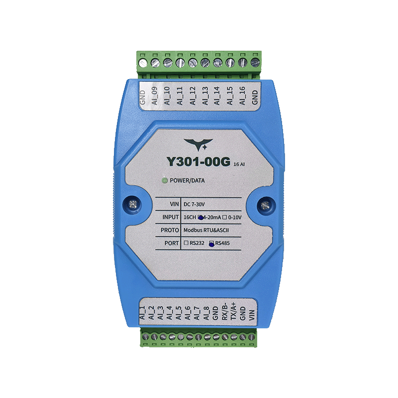
Appearance
Y301-006/008/00G Analog Input Module Technical Manual
| Y301-006 | Y301-008 | Y301-00G |
|---|---|---|
 | | |
Manufacturer: Hunan Yanji Tech Co.,Ltd
Address: Room 21014, Unit 1, Fudixingguang Plaza, Yuhua District Yingxin Road, Changsha, Hunan, P.R. China
Email: hi@yanjiiot.com
Website: www.yanjiiot.com
Table of Contents
- Introduction
- System Overview
- Wiring & Installation
- Modbus Communication Parameters
- Register Map
- Command Reference
- Configuration Workflow
- Diagnostics & FAQ
- Appendix
1. Introduction
This manual provides the Modbus integration details for the Y301-006/008/00G analog input modules (derived from DAM1600AI-YD hardware). The devices aggregate 4–20 mA or 0–10 V signals and publish the raw A/D values via RS485 or RS232 serial links. Content focuses on commissioning, wiring, register interpretation, and troubleshooting for engineers integrating the modules into PLC/SCADA systems.
Key facts from the original Chinese datasheet:
- Power: DC 7–30 V, single LED power indicator plus 16 channel LEDs.
- AI count: Y301-006 (6), Y301-008 (8), Y301-00G (16).
- Communication: Modbus RTU/ASCII over RS485 or RS232, 2400–38400 bps (9600 bps default).
- Actual value conversion:
Engineering Value = Register × 0.001.
2. System Overview
2.1 Hardware Summary
| Attribute | Detail |
|---|---|
| Enclosure | 100 × 70 × 35 mm, 35 mm DIN-rail |
| Supply Voltage | DC 7–30 V with reverse-polarity protection |
| Inputs | Opto-isolated AI terminals (AI1…AI16) plus COM |
| Indicators | 1 × POWER LED, 16 × AI LEDs mirroring live state |
| Environment | -40 °C ~ +85 °C, 5–95 % RH non-condensing |
2.2 Communication Summary
- RS485: A/B differential pair, shield recommended, up to 32 nodes on a daisy-chain bus (≤1200 m @ 9600 bps).
- RS232: TX/RX/GND point-to-point (≤15 m).
- Protocols: Modbus RTU (CRC-16) and Modbus ASCII (LRC).
- Addresses: Software offset only; there is no DIP switch. Effective slave address = offset address. Broadcast address = 254.
3. Wiring & Installation
3.1 Power & Communications
| Terminal | Description |
|---|---|
| VIN | 7–30 V DC positive |
| GND | 0 V return and shield reference |
| A / 485+ | RS485 positive line |
| B / 485- | RS485 negative line |
| TX | RS232 transmit (module → host) |
| RX | RS232 receive (host → module) |
- For RS485, use twisted-shielded pair, chain A-to-A and B-to-B, common the grounds, and terminate both ends with 120 Ω.
- For RS232, connect TX↔RX, RX↔TX, GND↔GND using straight-through wiring.
3.2 Analog Input Wiring
| Mode | Wiring Notes |
|---|---|
| 2-wire (loop powered) | Insert AI+ in series with the current loop. Sensor negative goes to COM. |
| 3-wire transmitter | Sensor OUT → AI+, sensor ground → COM, sensor +V → external supply. |
| 4-wire voltage source | Sensor Vout → AI+, sensor ground → COM. V_out pin on the module is unused. |
Important: Do not route both current and voltage outputs into the same channel simultaneously. Keep analog cables separate from high-voltage lines and connect shields at a single point.
4. Modbus Communication Parameters
| Parameter | Value |
|---|---|
| Default Format | 9600 bps, 8 N 1 |
| Supported Baud Rates | 2400 / 4800 / 9600 / 19200 / 38400 bps |
| Slave Address Range | 0–255 (0 unused, 254 broadcast) |
| Function Codes | 0x04 (read input registers), 0x03 (read holding), 0x06 (write single), 0x10 (write multiple for configuration) |
4.1 Broadcast Usage
- Set master to address 254 (0xFE) when only one device is on the bus to discover its actual address.
- When multiple devices are present, assign unique addresses; broadcast queries will cause bus contention.
4.2 Actual Value Conversion
A/D readings are 16-bit integers. Convert to engineering units using:
Actual Value (engineering units) = Register × 0.001Example: Register = 12345 → 12.345 units.
5. Register Map
5.1 Input Registers (Function 0x04)
| PLC Address | Modbus Offset | Channel | Description |
|---|---|---|---|
| 3x0001 | 0x0000 | AI1 | A/D result (counts) |
| 3x0002 | 0x0001 | AI2 | A/D result |
| … | … | … | … |
| 3x0010 | 0x000F | AI16 | A/D result (Y301-00G only) |
- Reading multiple channels returns contiguous values in ascending order.
- Each register is unsigned 16-bit. Apply the
×0.001scaling to obtain the field value.
5.2 Holding Registers (Function 0x03/0x06)
| PLC Address | Modbus Offset | Parameter | Notes |
|---|---|---|---|
| 4x1001 | 0x03E8 | Baud rate selector | 0–5 enumeration (see below) |
| 4x1002 | 0x03E9 | Reserved | Do not write |
| 4x1003 | 0x03EA | Offset/Slave address | Device address = offset |
Baud Rate Enumerations (per Chinese manual):
| Value | Baud |
|---|---|
| 0 | 9600 bps (default) |
| 1 | 2400 bps |
| 2 | 4800 bps |
| 3 | 9600 bps (legacy duplicate) |
| 4 | 19200 bps |
| 5 | 38400 bps |
Because the original PDF lists both 0 and 3 as 9600 bps, Yanji recommends using value 0 for the default and avoiding value 3 unless explicitly required by older firmware.
6. Command Reference
6.1 Read AI Channels (RTU)
| Use Case | Frame (hex) | Description |
|---|---|---|
| Read AI1 only | 01 04 00 00 00 01 31 CA | Query channel 1 |
| Read AI1–AI6 (Y301-006) | 01 04 00 00 00 06 70 08 | Returns 12 bytes |
| Read AI1–AI8 (Y301-008) | 01 04 00 00 00 08 F1 CC | Returns 16 bytes |
| Read AI1–AI16 (Y301-00G) | 01 04 00 00 00 10 70 0F | Returns 32 bytes |
Replace the first byte (01) with the actual slave address; use FE only when a single device is attached.
6.2 Address & Baud Configuration
| Action | Request (hex) | Notes |
|---|---|---|
| Read offset/slave address | 01 03 03 EA 00 01 75 D7 | Returns current address |
| Set address = 5 | 01 06 03 EA 00 05 88 0B | Write new offset |
| Read baud rate | 01 03 03 E8 00 01 14 17 | Returns enumeration value |
| Set baud = 19200 | 01 06 03 E8 00 04 D5 D7 | Power-cycle after writing |
6.3 Broadcast Example (single device only)
FE 04 00 00 00 08 6D C3Reads eight channels from the device currently on the bench; remove broadcast usage once multiple nodes share the bus.
7. Configuration Workflow
- Bench Setup
- Connect VIN/GND to a 12 or 24 V DC supply.
- Wire RS485 (A/B/GND) or RS232 (TX/RX/GND) to the host or USB converter.
- Open JYDAM or Modbus Master
- Set baud = 9600 bps, address = 254 (broadcast) to query the current offset.
- Once the actual slave ID is known, switch the master to that address.
- Assign Permanent Address
- Write the desired ID (1–255) to holding register 4×1003.
- Power-cycle or send a soft reset if firmware requires it.
- Verify Analog Acquisition
- Toggle sensor signals or inject known voltages/currents.
- Read channels using function 0x04; confirm engineering values via
×0.001.
- Finalize Baud/Protocol (Optional)
- Update 4×1001 for new baud, then restart.
- Keep RTU (binary) unless ASCII integration is mandatory.
8. Diagnostics & FAQ
| Symptom | Possible Cause | Recommended Action |
|---|---|---|
| RS232 link silent | TX/RX wiring incorrect or wrong baud | Use straight-through wiring RX↔RX, TX↔TX, verify baud/parity. |
| RS485 bus unstable | Multiple slaves still on broadcast address | Assign unique addresses, terminate bus ends, keep stubs <1 m. |
| AI reads zero | Open loop or voltage source not referenced | Check wiring to COM, ensure transmitter is powered, confirm range. |
| AI reads max value | Input wired to wrong mode or shorted to VIN | Validate sensor output type, inspect for short circuits. |
| Readings noisy/drifting | Shielding or grounding issues | Use shielded cable, single-point COM, separate power cabling. |
Common Questions
Q: Why does the software default to address 0 but Modbus address 0 is invalid?
A: The factory offset is 0, meaning the device must first be contacted via broadcast address 254. Set a non-zero offset (1–255) before deploying.Q: Is there any built-in scaling register?
A: No. The firmware only reports raw 12-bit data. Apply the×0.001multiplier on the host side to convert to engineering units.
9. Appendix
9.1 Field Commissioning Checklist
- Inspect power polarity and confirm POWER LED is lit.
- Measure RS485 A/B polarity and confirm shield continuity.
- Use broadcast read to verify raw data toggles when sensor is stimulated.
- Write permanent address, reboot, and retest.
- Document register snapshots and sensor wiring for maintenance logs.
9.2 Error Codes
| Code | Meaning |
|---|---|
| 0x01 | Illegal function |
| 0x02 | Illegal data address |
| 0x03 | Illegal data value |
| 0x04 | Slave device failure |
Exception responses echo the request with function code + 0x80 and append the code above.
- Manufacturer: Hunan Yanji Tech Co.,Ltd
- Address: Room 21014, Unit 1, Fudixingguang Plaza, Yuhua District Yingxin Road, Changsha, Hunan, P.R. China
- Email: hi@yanjiiot.com
- Website: www.yanjiiot.com