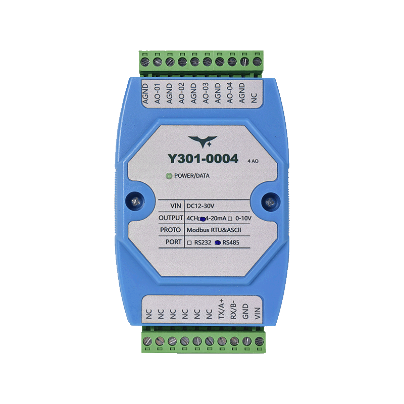
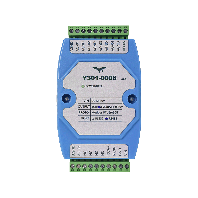
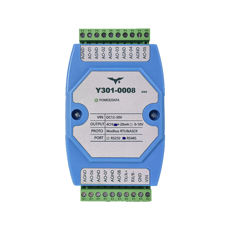
Appearance
Y301-0004/0006/0008 Analog Output Module Technical Manual
| Y301-0004 | Y301-0006 | Y301-0008 |
|---|---|---|
 |  |  |
Manufacturer: Hunan Yanji Tech Co.,Ltd
Address: Room 21014, Unit 1, Fudixingguang Plaza, Yuhua District Yingxin Road, Changsha, Hunan, P.R. China
Email: hi@yanjiiot.com
Website: www.yanjiiot.com
Table of Contents
- Introduction
- System Overview
- Interfaces & Wiring
- Modbus Communication Parameters
- Register Map
- Command Reference
- Configuration Workflow
- Diagnostics & FAQ
- Appendix
1. Introduction
This manual explains how to commission and integrate the Y301-0004/0006/0008 analog output modules (based on the DAM0800AO-YD platform). These devices present up to eight 14-bit DAC channels over Modbus RTU/ASCII, allowing PLCs, SCADA systems, or industrial PCs to drive voltage (0–10 V) or current (4–20 mA) loops.
Highlights from the original Chinese manual:
- 12–30 V DC supply, RS485 optical isolation, RS232 optional.
- 14-bit resolution with ±0.03 % FS accuracy at 25 ° C.
- Output code mapping:
Actual Value = Register × 0.001(V or mA). - Baud rates: 2400–115200 bps (default 9600).
- Broadcast address 254 for commissioning; address = offset (no DIP switches).
2. System Overview
2.1 Hardware Summary
| Attribute | Detail |
|---|---|
| Enclosure | 100 × 70 × 35 mm, DIN-rail mounting |
| Power | 12–30 V DC (reverse-polarity tolerant) |
| Outputs | AO1…AO8 positives plus AGND return |
| Indicators | Per-channel AO LEDs, POWER LED |
| Output Modes | 0–10 V, 4–20 mA, or jumper-selectable combination |
| Memory | Optional power-off retention for channel values |
2.2 Communication Summary
- RS485 (A/B/GND) with optical isolation for multi-drop buses.
- RS232 (TX/RX/GND) for point-to-point setups.
- Modbus RTU and ASCII are native; Modbus TCP supported via gateways.
- Slave address range 1–255; broadcast 254 for temporary discovery; address 0 invalid.
3. Interfaces & Wiring
3.1 Pinout
| Group | Terminal | Description |
|---|---|---|
| Power | VCC | 12–30 V DC positive |
| Power | GND | 0 V return |
| Serial | RX / B- | RS232 RX or RS485 B- |
| Serial | TX / A+ | RS232 TX or RS485 A+ |
| Analog Output | AO1…AO8 | Channel positives |
| Analog Output | AGND | Common analog return |
Compatible SKUs expose internal jumper headers to toggle each channel between voltage and current mode. Non-compatible SKUs are fixed 0–10 V or 4–20 mA as ordered.
3.2 Voltage Output Wiring
- Connect AOx to the receiving device’s voltage input (+).
- Tie AGND to the receiving device’s analog ground.
- Ensure input impedance ≥10 kΩ for minimal loading.
3.3 Current Output Wiring
- Loop AOx through the target 4–20 mA input (AOx → PLC AI+, PLC AI− → AGND).
- Provide loop power if the PLC input is passive.
- Maintain correct polarity to avoid saturating at 0 mA.
3.4 Communication Cabling
- RS485: Twisted-shielded pair, daisy-chain topology, 120 Ω termination at both ends, shield bonded to GND at one point only.
- RS232: Straight-through cable (TX↔RX, RX↔TX, GND↔GND) up to 15 m.
- USB–RS485 adapters are recommended for PCs; choose isolated models for industrial sites.
4. Modbus Communication Parameters
| Parameter | Value |
|---|---|
| Default UART | 9600 bps, 8 data bits, no parity, 1 stop bit |
| Baud Rate Codes | 0:9600, 1:2400, 2:4800, 3:9600, 4:19200, 5:38400, 6:115200, 7:57600, 8:56000, 9:14400, 10:1200 |
| Parity Codes | 0:none, 1:even, 2:odd |
| Stop Bits | 0:1 bit, 1:2 bits, 2:1.5 bits |
| Function Codes | 0x03 (read AO registers), 0x06 (single write), 0x10 (multi-write), 0x04 (internal diagnostics) |
4.1 Output Scaling
Write Code = Desired Value × 1000
Actual Value = Register × 0.001
Examples:
- 5.000 V → write 5000.
- 12.5 mA → write 12500.
- 0 V corresponds to code 0; 4 mA corresponds to 4000.
4.2 Broadcast Usage
- Use slave address 0xFE (254) only when a single device is connected.
- With multiple nodes on an RS485 bus, assign unique addresses immediately to avoid collisions.
5. Register Map
5.1 Analog Output Registers
| Channel | PLC Address | Modbus Offset | Description |
|---|---|---|---|
| AO1 | 4x0001 (u160) | 0x0000 | Output code for channel 1 |
| AO2 | 4x0002 (u161) | 0x0001 | Output code for channel 2 |
| AO3 | 4x0003 (u162) | 0x0002 | Output code for channel 3 |
| AO4 | 4x0004 (u163) | 0x0003 | Output code for channel 4 |
| AO5 | 4x0005 (u164) | 0x0004 | Output code for channel 5 (0006/0008 only) |
| AO6 | 4x0006 (u165) | 0x0005 | Output code for channel 6 (0006/0008 only) |
| AO7 | 4x0007 (u166) | 0x0006 | Output code for channel 7 (0008 only) |
| AO8 | 4x0008 (u167) | 0x0007 | Output code for channel 8 (0008 only) |
- Read/write operations: Function 0x03 for reading current outputs, 0x06 for single-channel writes, 0x10 for batch writes.
5.2 Configuration Registers
| PLC Address | Modbus Offset | Parameter | Notes |
|---|---|---|---|
| 4x1000 | 0x03E8 | Serial format enumeration (baud/parity/stop bits) | |
| 4x1001 | 0x03E9 | Reserved | |
| 4x1002 | 0x03EA | Offset/slave address | |
| Additional | — | Dropout memory, mode selection | Accessed via JYDAM (implementation-specific) |
Serial format word combines baud, parity, and stop bits (see Section 4.0). Use JYDAM “Configuration Parameters” panel or write the bit field manually.
6. Command Reference
6.1 Typical RTU Frames
| Use Case | Request (hex) | Description |
|---|---|---|
| Query AO1 | 01 03 00 00 00 01 84 0A | Reads channel 1 code |
| Query AO1–AO4 | 01 03 00 00 00 04 45 CA | Reads four outputs |
| Write AO1 = 5 V | 01 06 00 00 13 88 8C CB | 5.000 V → 5000 (0x1388) |
| Write AO1 = 12 mA | 01 06 00 00 2E E0 A5 0C | 12.000 mA → 12000 |
| Write AO1–AO8 simultaneously | 01 10 00 00 00 08 10 … CRC | Function 0x10 with 16 data bytes |
| Read slave address | 01 03 03 EA 00 01 75 D7 | Returns offset register |
| Set address = 7 | 01 06 03 EA 00 07 48 0C | Writes offset register |
Replace the leading byte (01) with the actual slave ID. Use FE only for single-device commissioning.
6.2 Broadcast (Address 254) Multi-Write
FE 10 00 00 00 08 10 [16 bytes data] CRCAll connected devices receive the same output codes. Do not use when multiple nodes must maintain unique values.
7. Configuration Workflow
- Power & Wiring
- Supply 12–30 V DC, verify POWER LED.
- Wire RS485 (A/B/GND) or RS232 (TX/RX/GND).
- Connect analog outputs to the target loads (voltage or current mode).
- Initial Communication
- Use JYDAM or a Modbus master at 9600 bps, address 254 to identify the device.
- Read register 0x03EA to confirm current slave address.
- Assign Address & Serial Format
- Write the desired address to 0x03EA.
- Update baud/parity/stop bits via 0x03E8 if non-default settings are required, then reboot.
- Set Outputs
- Convert engineering values to codes (
Value × 1000). - Use function 0x06 or 0x10 to write channels; confirm with a readback.
- Convert engineering values to codes (
- Enable Dropout Memory (if supported)
- Through JYDAM, enable “Power-Off Memory” so outputs resume last values after restart.
8. Diagnostics & FAQ
| Symptom | Root Cause | Solution |
|---|---|---|
| No response via RS232 | TX/RX swapped or wrong serial settings | Check straight-through wiring, ensure baud/parity matches register 0x03E8. |
| AO writes succeed but outputs stay at zero | Wrong output mode (jumpers) or AGND not referenced | Verify voltage/current jumper positions, confirm AGND connection to PLC reference. |
| Output jitter/noise | Load impedance too low or wiring near high-noise bundles | Keep load ≥10 kΩ (voltage mode), route analog cables away from relays/VFDs. |
| RS485 bus collisions | Multiple devices left on address 1 or broadcast 254 | Assign unique addresses immediately after commissioning. |
| Software shows “communication success” but no physical output | Value written outside valid range (0–10000 or 4000–20000) | Clamp values before writing; confirm firmware expects raw codes. |
9. Appendix
9.1 Quick Reference Table
| Mode | Code Range | Engineering Range |
|---|---|---|
| Voltage (0–10 V) | 0–10000 | 0.000–10.000 V |
| Current (4–20 mA) | 4000–20000 | 4.000–20.000 mA |
9.2 Troubleshooting Checklist
- Verify supply voltage and LED indicators.
- Check Modbus address via broadcast read.
- Confirm baud/parity configuration matches master.
- Inspect analog wiring and jumper configuration.
- Use a multimeter or PLC diagnostics to confirm output magnitude.
- If problems persist, contact Yanji support (400-668-8400) with register dumps and wiring photos.
- Manufacturer: Hunan Yanji Tech Co.,Ltd
- Address: Room 21014, Unit 1, Fudixingguang Plaza, Yuhua District Yingxin Road, Changsha, Hunan, P.R. China
- Email: hi@yanjiiot.com
- Website: www.yanjiiot.com